STORY HIGHLIGHTS
- Graphene is the world's first two-dimensional material to be discovered
- No material is stronger, thinner or more conductive than graphene
- MIT professor Tomas Palacios says graphene will change all our lives
- Numerous applications for graphene in fields of computing, energy and medicine
By Eoghan Macguire and Matthew Knight, CNN
(CNN) -- Ever since it was discovered in 2004, graphene has been hailed as a natural wonder of the materials world destined to transform our lives in the 21st century.
Graphene's amazing properties excite and confound in equal measure. How can something one million times thinner than a human hair be 300 times stronger than steel and 1,000 times more conductive than silicon?
CNN Labs asked the head of MIT's graphene research department, Tomas Palacios, to explain why graphene is such a special material and what we can expect it to do for us in the future.
CNN: What is graphene?
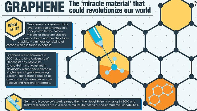
Tomas Palacios (TP): Graphene is a one-atom thick layer of carbon atoms arranged in a honeycomb lattice.
This special atomic arrangement gives graphene truly unique properties. For example electrical currents in graphene move faster than in any other material we know of.
Products such as cell-phones will be integrated into the likes of the clothes, pieces of paper and in windows
Tomas Palacios
Tomas Palacios
Heat can also move in graphene very fast and it is the best thermal conductor that we have. On top of this, graphene is the thinnest material in the world as well as the strongest, much stronger than steel and, of course, much lighter.
Finally, because it is only one atom thick, it is perfectly transparent and flexible.
CNN: What applications will it have?
TP: The very first application where graphene is going to be used is probably as a replacement for (the relatively expensive metal) indium selenide in solar cells.
After that, I think we will see a new array of communication devices that don't just use graphene but which also use other two-dimensional materials.
Products such as cell phones will be integrated into the likes of the clothes, pieces of paper and in windows.
Another direction is transparent displays. Basically we are going to have electronic displays embedded almost everywhere, in the windows, in our glasses, in the walls, everywhere.
To do this we need very thin materials that are also transparent and graphene could be that material.
CNN: When will products containing graphene be available?
TP: It depends on the specific application. I believe that the use of graphene in solar cells, displays and so on is probably going to be in the marketplace in a couple of years.
More complex applications such as computers or cell phones will probably take longer, maybe within five and ten years.
CNN: What challenges remain for researchers?
TP: One important challenge facing graphene is the way the material is developed.
Graphene was isolated for the first time using the Scotch Tape technique (where ever thinner strips are peeled off a block of graphite using sticky tape) and the quantities we can make in large areas still lag behind this method.
The ambition is that one day graphene will be fabricated in the same way that you print newspapers
Tomas Palacios
Tomas Palacios
There has been a lot of work to try and enhance the manufacturability of graphene and there are a few techniques that look very promising but they are not completely mature yet.
The second challenge is that graphene is a material that is only one atom thick. Anything that you do to it is going to impact its properties.
We still need to understand better how to fabricate graphene devices and how to be gentle enough not to (break) the formula.
CNN: Are production methods improving?
Recently, Samsung Electronics has demonstrated a single layer of graphene which is 30 inches in diameter. So in just a few years we have gone from micro-meter sized flakes all the way to 30 inches.
The ambition is that one day graphene will be fabricated in the same way that you print newspapers -- in a roll to roll process using the same kind of equipment. This will change the entire economics of the electronics industry.
CNN: Are there any other materials like graphene?
TP: Graphene was the first two-dimensional material to be discovered, but it is not the only one. Now there are more than 10 materials that are all two-dimensional with complimentary properties that could be integrated with graphene to provide extra functionality.
Boron nitride for example is also one-atom thick and instead of being a conductor it is an insulator (of heat), the best insulator we know. If you go to three atoms thick we have another material called molybdenum disulfide which is a semi-conductor, like silicon, but lighter and stronger.
These materials can then be combined in order to fabricate completely new material structures that don't exist in nature. I think that that is a very powerful proposition.
I am completely convinced that graphene is going to end up changing our lives
Tomas Palacios
Tomas Palacios
CNN: When will graphene-based products hit main street?
TP: If you look at how long it traditionally takes new materials to make an impact in the market, it typically takes around 20 years.
We need to be patient but things seem to be moving faster than with other materials.
I think the next couple of years will see quite significant improvements in the growth techniques and synthesis of two-dimensional materials.
At a basic research level we are going to see an emphasis on trying to understand what happens when you stack these materials one on top of the other.
That is going to enable a lot of new understanding which will enable completely new devices.
I am completely convinced that graphene is going to end up changing our lives. Exactly how, I don't know and I don't think anyone can know for sure but there is nothing thinner, stronger or more suitable to conduct electricity and that has to be useful for many important things.
Fonte: CNN