Pesquisar este blog

Translate

quinta-feira, 17 de dezembro de 2015

Nanotecnologia no agro: conheça o plástico para comer

Película desenvolvida por cientistas permite que alimentos tenham uma vida útil mais longa e que possam ser ingeridos por seres humanos

 article-_creditoflavioubiali
Tecnologias de ponta aplicadas ao agronegócio já geraram inúmeras invenções que beneficiam o consumidor final. Neste ano, uma das maiores descobertas anunciadas no Brasil foi a criação de um filme plástico que pode ser ingerido pelos seres humanos.
A descoberta foi de pesquisadores da Rede de Nanotecnologia Aplicada ao Agronegócio (AgroNano), da Embrapa. Eles desenvolveram um produto comestível produzido a partir de alimentos como espinafre, mamão, goiaba e tomate.
As características do plástico– resistência, textura, capacidade de proteção – são parecidas às de um papel-filme convencional. De acordo com Luiz Henrique Capparelli Mattoso e José Manoel Marconcini, coordenadores da pesquisa, as matérias-primas usadas passaram pelo processo de liofilização, um tipo de desidratação em que, após o congelamento do alimento, toda a água contida é transformada em sólido diretamente gasoso, sem passar pela fase líquida.
O resultado é um alimento completamente desidratado, mas com propriedades nutritivas. O processo, segundo eles, pode ser feito com frutas, verduras, legumes e até alguns temperos.

Na Embrapa, o plástico ainda teve adicionado à sua fórmula a quitosana, um polissacarídeo presente na carapaça de caranguejos com propriedades bactericidas e isso, segundo os pesquisadores, aumenta o tempo de prateleira dos alimentos.

segunda-feira, 14 de dezembro de 2015

7 Ways Nanotechnology Could Provide The Solutions To Combat Climate Change

This week we saw global leaders come together in Paris, with the goal of reaching a new international agreement on climate change, applicable to all, to keep global warming below 2°C. The United Nations Framework Convention on Climate Change is aiming to keep global temperature rises comparable to pre-industrial levels and adapt our societies to existing disruption, and nanotechnology will be one of the key sciences in order to enable and disrupt to make this goal a reality. 

Here we look at the 7 ways that nanotechnology can help to combat and possibly stop climate change.


1. Lightweight nano-composite materials - Any effort to reduce emissions in vehicles by reducing their weight , in turn, decreasing fuel consumption can have an immediate and significant global impact. It is estimated that a 10% reduction in weight of the vehicle corresponds to a 10% reduction in fuel consumption, leading to a proportionate fall in emissions. In recognition of the above, there is growing interest worldwide in exploring means of achieving weight reduction in automobiles through use of novel materials. For example, use of lighter, stronger, and stiffer nano-composite materials is considered to have the potential to significantly reduce vehicle weight. 


2. Nano-coatings - Nanotechnology coatings are a good short-term way of reducing emissions and and maximizing clean energy production. For example, nano-coatings can be applied to aircraft, which can make aircraft's smoother, reducing drag and also protect the materials from the special conditions of the environment where they are used (instead of the conventional bulk metals such as steel). Since the amount of CO2 emitted by an aircraft engine is directly related to the amount of fuel burned, CO2 can be reduced by making the airplane lighter. Hydrophobic nano-coatings can also improve the energy produced from solar panels for example.


3. Nanocatalysts - Nanotechnology is already applied to improve fuel efficiency by incorporation of nanocatalysts. Enercat, a third generation nanocatalyst developed by Energenics, uses the oxygen storing cerium oxide nanoparticles to promote complete fuel combustion, which helps in reducing fuel consumption. Recently, the company has demonstrated fuel savings of 8%–10% on a mixed fleet of diesel vehicles in Italy. Reducing friction and improving wear resistance in engine and drive train components is of vital importance in the automotive sector. Based on the estimates made by a Swedish company Applied Nano Surfaces, reducing friction can lower the fuel consumption by about 2% and result in cutting down CO2 emissions by 500 million tons per year from trucks and other heavy vehicles in Sweden alone.


4. Nano-structured Materials - Thanks to nanomaterials like silica, many tires will in the future be capable of attaining the best energy rating, the green category. Cars equipped with category A tires consume approximately 7.5% less fuel than those with tires of the minimum standard (category G). Residential and commercial buildings contribute to 11% of total greenhouse gas emissions. Space heating and cooling of residential buildings account for 40% of the total residential energy use. Nanostructured materials, such as aerogels, have the potential to greatly reduce heat transfer through building elements and assist in reducing heating loads placed on air-conditioning/heating systems. Aerogel is a nanoporous super-insulating material with extremely low density; silica aerogel is the lightest solid material known with excellent thermal insulating properties, high temperature stability, very low dielectric constant and high surface area.

5. Improved Renewables - Nanotechnology may accelerate the technology behind renewables in various ways:experts are discovering means to apply nanotechnology to photovoltaics, which would produce solar panels with double or triple the output by 2020; wind turbines stand to be improved from high-performance nano-materials like graphene, a nano-engineered one-atom thick layer of mineral graphite that is 100 times stronger than steel. Nanotechnology will enable light and stiff wind blades that spin at lower wind speeds than regular blades;nanotechnology could play a major role in the next generation of batteries. For example, coating the surface of an electrode with nanoparticles increases the surface area, thereby allowing more current to flow between the electrode and the chemicals inside the battery. 

6. Batteries - Such techniques could increase the efficiency of electric and hybrid vehicles by significantly reducing the weight of the batteries. Nanotechnology is positioned to create significant change across several domains, especially in energy where it may bring large and possibly sudden performance gains to renewable sources and Smart Grids. Nanotech enhancements may also increase battery power by orders of magnitude, allowing intermittent sources such as solar and wind to provide a larger share of overall electricity supply without sacrificing stability.

Moreover, superior batteries would complement renewables by storing energy economically, thus offsetting the whole issue of intermittent generation.In a somewhat more distant future, we may see electricity systems apply nanotechnology in transmission lines. Research indicates that it is possible to develop electrical wires using carbon nanotubes that can carry higher loads and transmit without power losses even over hundreds of kilometers. The implications are significant, as it would increase the efficiency of generating power where the source is easiest to harness. Semiconductor devices, transistors, and sensors will benefit from nanotechnology especially in size and speed. 

7. Nanotech sensors - Sensors could be used for the Smart Grid to detect issues ahead of time, ie, to measure degrading of underground cables or to bring down the price of chemical sensors already available for transformers. Nanotechnology will likely become indispensable for the Smart Grid to fully evolve in the near future. Energy efficiency is a way of managing and restraining the growth of energy consumption. It is one of the easiest and most cost effective ways to combat climate change, improve the competitiveness of businesses, and reduce energy costs for consumers.


The Economist: The Fourth Industrial Revolution will be battery powered

Material difference
Materials science is rapidly transforming the way that everything from cars to light bulbs is made, says Paul Markillie
“I DO not depend on figures at all,” said Thomas Edison. “I try an experiment and reason out the result, somehow, by methods which I could not explain.” And so it was that by testing 1,600 different materials, from coconut fibre to fishing line and even a hair from a colleague’s beard, Edison finally found a particular type of bamboo which could be used, in carbonised form, as the filament in the first proper incandescent light bulb. He demonstrated it on New Year’s Eve 1879 at his laboratory in Menlo Park, New Jersey.

The details of all this painstaking trial and error filled more than 40,000 pages of Edison’s notebooks, but his solution was soon superseded. By the start of the 20th century filaments were being made from tungsten, which burned brighter and lasted longer. For over 100 years the world was illuminated by light bulbs with tungsten filaments, and the light bulb became the cartoonist’s fixed shorthand for innovation of all sorts.

Now light bulbs are being replaced by light-emitting diodes (LEDs), which are more efficient at turning electricity into light than filaments are, and far longer-lived. LEDs first appeared in the 1960s as indicator lights on electrical equipment. Today they provide powerful illumination for buildings, streets and cars. In poor parts of the world they are bringing light to people who have never seen an old-fashioned bulb.

Both Edison’s light bulb and the LED are inventions of materials science, the process of turning matter into new and useful forms. But in the years between them both the materials and the science became much more complex. The semiconducting materials, such as germanium or silicon, from which LEDs are made, often with the careful addition of atoms of some other substance, require a different approach from that at Menlo Park. The sort of light they produce is fine-tuned by microscopic structures and the details of those extra atoms. Pace Edison, this sort of thing depends on a lot of figures—not to mention quantum theory.

The ability to understand the properties of materials at the tiniest scales not only lets people do old things better; it lets them do new things. In Edison’s day, using light to send messages was the province of the Aldis lamps that flashed messages in morse code from ship to ship. Laser diodes—semiconductor devices engineered to produce a much purer light than LEDs—can flicker on and off in a controlled way billions of times a second. In an astounding number of applications where information has to get from A to B—be those end points a DVD and a speaker, a bar code and a supermarket checkout or the two ends of a transatlantic fibre-optic cable—laser diodes are doing the work. For all its seeming abstraction, the virtual world is built on very real, very well-understood materials.

The warp and weft of a new car

This is what some scientists describe as a “golden age” for materials. New, high-performing substances such as exotic alloys and superstrong composites are emerging; “smart” materials can remember their shape, repair themselves or assemble themselves into components. Little structures that change the way something responds to light or sound can be used to turn a material into a “metamaterial” with very different properties. Advocates of nanotechnology talk of building things atom by atom. The result is a flood of new substances and new ideas for ways of using them to make old things better—and new things which have never been made before.

University materials departments are flourishing, spawning a vibrant entrepreneurial culture and producing a spate of innovations (see box below). Many of these discoveries will fail to scale up from laboratory demonstration to commercial proposition. But some just might change the world, as light bulbs did.

Faster, higher, stronger

The understanding of the material world provided by a century of physics and chemistry accounts for much of the ever-accelerating progress. But this is not a simple triumph of theory. Instruments matter too. Machines such as electron microscopes, atomic-force microscopes and X-ray synchrotrons allow scientists to measure and probe materials in much greater detail than has ever been possible before.

A project at the International Centre for Advanced Materials at the University of Manchester shows such advances in action. In one of its labs scientists are using secondary ion mass spectrometry (SIMS) to study the way that hydrogen atoms—the smallest atoms there are—diffuse into materials such as steel, a process that can cause tiny cracks. SIMS works by bombarding a sample with a beam of charged particles, which causes secondary particles to be ejected from the surface. These are measured by an array of detectors to create an image with a resolution down to 50 nanometres (billionths of a metre). It does not just reveal the crystalline structure of the metal—and any flaws in it—but also determines chemical impurities, such as the presence of hydrogen. “We can now do in an afternoon what we once did in months,” says Paul O’Brien, a professor at the university. The hope is that BP, the oil company which is sponsoring the centre, will get better steels for its offshore and processing work as a result.

As well as having ever better instruments, the researchers are also benefiting from a massive increase in available computing power. This allows them to explore in detail the properties of virtual materials before deciding whether to try and make something out of them.

“We are coming out of an age where we were blind,” says Gerbrand Ceder, a battery expert at the University of California, Berkeley. Together with Kristin Persson, of the Lawrence Berkeley National Laboratory, Mr Ceder founded the Materials Project, an open-access venture using a cluster of supercomputers to compile the properties of all known and predicted compounds. The idea is that, instead of setting out to find a substance with the desired properties for a particular job, researchers will soon be able to define the properties they require and their computers will provide them with a list of suitable candidates.

Their starting point is that all materials are made of atoms. How each atom behaves depends on which chemical element it belongs to. The elements all have distinct chemical properties that depend on the structure of the clouds of electrons that make up the outer layers of their atoms. Sometimes an atom will pair off one of its electron with an electron from a neighbouring atom to form a “chemical bond”. These are the kind of connections that give structure to molecules and to some sorts of crystalline material, such as semiconductors. Other sorts of atom like to share their electrons more widely. In a metal the atoms share lots of electrons; there are no bonds (which makes metals malleable) and electric currents can run free.

When it comes to making chemical bonds, one element, carbon, is in a league of its own; a more or less infinite number of distinct molecules can be made from it. Chemists call these carbon-based molecules organic, and have devoted a whole branch of their subject—inorganic chemistry—to ignoring them. Mr Ceder’s Materials Project sits in that inorganic domain. It has simulated some 60,000 materials, and five years from now should reach 100,000. This will provide what the people working on the project call the “materials genome”: a list of the basic properties—conductivity, hardness, elasticity, ability to absorb other chemicals and so on—of all the compounds anyone might think of. “In ten years someone doing materials design will have all these numbers available to them, and information about how materials will interact,” says Mr Ceder. “Before, none of this really existed. It was all trial and error.”
Latest discoveries

Curiouser and curiouser

IN the month of November 2015 alone, materials scientists alerted the media to more than 100 significant discoveries. Here is a small selection from the professional journals:

  • • A type of crystal called a perovskite can be used to make light-emitting diodes that glow exceptionally bright. These could be used in lighting and displays. Hanwei Gao and Biwu Ma of Florida State University.Advanced Materials.
  • • Experiments with an exotic form of electronics called “valleytronics”, named after one of the ways in which electrons can move through a semiconductor, shows that the technology might be used to make ultra-low-power computers. Seigo Tarucha and colleagues at the University of Tokyo. Nature Physics.
  • • Quantum dots made from nanoparticles of iron pyrite, commonly known as fool’s gold, could help batteries charge up much faster. Cary Pint, Anna Douglas and colleagues at Vanderbilt University, Nashville.ACS Nano.
  • • Biosensors made from graphene can provide high levels of sensitivity to help speed up the development of new drugs. Aleksey Arsenin and Yury Stebunov of the Moscow Institute of Physics and Technology. ACS Applied Materials and Interfaces.
  • • Materials called microwave absorbers are used to make detection by radar of objects such as stealth fighters more difficult. A new lightweight material with arrays of patterned conductors would greatly improve cloaking properties. Wenhua Xu and colleagues of Huazhong University of Science and Technology, China. Journal of Applied Physics.
  • • A new class of “porous liquid”, which features permanent holes at the molecular level, could provide a number of practical applications, including capturing carbon-dioxide emissions from factories. Stuart James and colleagues at Queen’s University Belfast. Nature.
  • • Voltage-sensitive nanomaterials could be inserted into human tissue to gather information about how the brain functions and help diagnose injury and disease. James Delehanty and colleagues at the US Naval Research Laboratory, Washington, DC. NANO Letters.

A walk through the labs of General Electric (GE)—the firm into which Edison’s trial-and-error-based businesses were merged in 1892—shows similar approaches already in practice. Michael Idelchik, the head of GE Research, points to new artificial garnets developed for use in body scanners. The scanners have to turn X-rays into visible light to create images, and the better they do so the lower the dose of X-rays the patient is exposed to. The company looked at 150,000 subtly different types of crystal that scintillate when subjected to X-rays before settling on a specific type of garnet which, it hopes, will make scans much faster—safer and more pleasant for the patient, more cost-effective for the hospital.

On top of the possibilities offered by single materials comes the potentially even richer world of combining them. Elsewhere in Mr Idelchik’s empire work focuses on replacing nickel-alloy parts for jet engines with parts made from ceramic-matrix composites (CMCs). Their strong chemical bonds mean ceramics can endure more heat than metals; at the same time, and for related reasons, they are more brittle. A CMC that combines a metal with a ceramic—GE is using silicon carbide—can get you the best of both worlds. The company hopes CMCs that need less cooling will mean more efficient engines that emit less carbon dioxide.

Computing power helps create such hybrids. It also helps designers understand how such novel materials can best be used. Many prototypes are now produced in virtual form long before a physical item is made, using software from companies such as Altair, a Michigan firm, Autodesk, a Californian one (see the “Brain scan” interview later in this report), and Dassault Systèmes, a French group. Engineers can model a chemicals plant, architects can “walk” clients through a digital representation of a building, and cars can be virtually test-driven on different roads and parked alongside rivals’ vehicles in street scenes.

All this greatly speeds up product development. The software is powerful enough to take the properties of the materials used into account, allowing it to calculate things such as loads, stresses, fluid dynamics, aerodynamics, thermal conditions and much more.

Manufacturers are only just beginning to realise the potential this offers, says Jeff Kowalski, chief technology officer of Autodesk. Many firms simply adapt parts to use new materials, expecting to produce them with the same tools and processes as before. That gives “substandard results”, he reckons. It is when new materials are used to redefine production processes and enable wholly new types of product that things get really innovative, and cartoonists get to draw light bulbs over people’s heads.

Just the thing

Business is heading towards a world of “generative design”, says Mr Kowalski: engineers will set out what they want to achieve and the computer will provide designs to fit that purpose. As materials knowledge grows, computers will also find materials to meet the properties specified by a designer. The properties of materials may even vary throughout their length and breadth, because it is becoming easier to tinker with the microstructure. Some companies are already well on their way to offering such Savile Row tailoring of materials.Nanoparticles: To the heart of the matterEngineering at the molecular level improves old materials as well as creating new ones

NANOPARTICLES are often seen as a new, man-made invention, but they have long existed in nature—salt from the sea and smoke from volcanoes can be found in the atmosphere in the form of nanoparticles. What interests materials scientists is that with modern processing techniques it is possible to turn many bulk materials into nanoparticles—measured as 100 nanometres (billionth of a metre) or less. The reason for doing so is that nanoparticles can take on new or greatly enhanced properties because of quantum mechanics and other effects. This includes unique physical, chemical, mechanical and optical characteristics which are related to the particles’ size. Engineers can capture some of those properties by incorporating nanoparticles into their materials.

Nanoparticles can take on new or greatly enhanced properties
Christina Lomasney, a physicist, is using nanoparticles to make nanolaminates, a completely new class of material. She is the co-founder of Modumetal, a Seattle firm developing a type of electrolytic deposition. This works a bit like electroplating, in which a metal, usually in a salt form, is suspended in a liquid and deposits itself on a component when an electric current is applied.

Modumetal has come up with a way to do this with great precision, using a variety of metals in the liquid. By carefully manipulating the electric field, it builds up veneers of different metals over a surface and controls how those layers interact with one another. “In effect, we grow a material, controlling its composition and microstructure,” says Ms Lomasney. The company reckons it can do this at an industrial scale, cheaply and with conventional materials, such as steel, zinc and aluminium.

Its first products—various pumps, valves and fasteners—are treated with corrosion-resistant layers that are more durable than conventional treatments, lasting up to eight times longer. Some of them are already being used by oil and gas companies. Modumetal is now expanding production and, in time, plans not just to coat structures but actually grow them.

One of the more important applications for engineering the microstructure of materials is in batteries. These have been made from various materials, such as lead-acid and nickel-cadmium. Apart from being highly toxic, some of these ingredients are also bulky and heavy, hence mobile phones in the 1980s were brick-like. The rechargeable lithium-ion battery helped slim them down.
Scientists had been working on using lithium as a battery material for decades, because it is light and highly conductive. The difficult bit was shifting from the laboratory to large-scale production. Lithium is inherently unstable, so instead of using the material in its metallic form, researchers turned to safer compounds containing lithium ions. In 1991 Sony successfully launched a commercial version of the lithium-ion battery, helping transform portable consumer electronics.

Such batteries now power all manner of devices, not just smartphones and laptops but also power tools, electric cars and drones. Manufacturing faults and overcharging can cause them to overheat and even burst into flames, but after a series of early laptop-battery recalls and a number of fires in cars and aircraft, manufacturers now seem to have got on top of these problems.

Yet the search for a better battery is still on. For some applications, such as electric cars, this would be transformative. Until recently the battery for an electric car could cost $400-$500 per kilowatt hour, representing perhaps 30% or so of the overall cost of the vehicle, but costs are falling (see chart). In October General Motors said it expected the battery in its new Chevy Bolt electric car, due to go on sale in 2016, to cost around $145 per kilowatt hour. The industry believes that once the cost comes down to around $100 per kilowatt hour, electric vehicles will become mainstream because they will be able to compete with petrol cars of all sizes without subsidy.


Getting there will require some clever materials science. Lithium-ion batteries are usually made as a laminated structure with a material called an electrolyte at their centre, typically a liquid or gel-like substance through which the lithium ions shuttle back and forth between electrodes.

Tesla's bright idea

Lithium-ion batteries have been steadily getting better. Jeffrey “JB” Straubel, chief technology officer of Tesla, a Californian maker of electric cars, says that the battery cells for the company’s present Model S are made on equipment similar to that used a decade ago for the firm’s first car, the Roadster. But with improved chemistry and production techniques, the energy stored in them has increased by 50%. Tesla has teamed up with its Japanese battery supplier, Panasonic, to build a $5 billion factory in Nevada that should push car-battery costs lower. It will also make a new Tesla battery called Powerwall (pictured), which can be used to store solar electricity generated at home.

Lay it on thin

Other companies are looking at a more radical change in the technology. One of them is Sakti3, a Michigan startup, which is trying to commercialise a lithium-ion battery with a solid electrolyte. Solid-state lithium batteries already exist, but mostly in the form of coin-sized back-ups in electrical circuits. Scaling up production processes to make them big enough to power devices such as phones would be hideously expensive.

Sakti3, however, has found a way to make a solid lithium battery with a thin-film deposition process, a technique already widely used to produce things such as solar panels and flat-panel display screens. “Solid-state technology will offer about double the energy density—that’s double the talk time on your phone; double the range in your electric car,” says Ann Marie Sastry, the firm’s chief executive. The battery cells will also have a long service life and be safer, she adds.

So why has the technique not been used to make batteries before? The firm’s purported edge is knowing what materials to use and how to make the process cost-effective. Everything, including the complicated physics, was worked out and extensively tested virtually before the company built a pilot production line. Ms Sastry explains that as the firm selected materials and developed processes, the virtual computer tests enabled it to forecast the cost of scaling up production. When built in large volumes, the solid-state batteries should come in around $100 per kilowatt hour, and there is scope for further improvement.

Initially Sakti3 expects its solid-state cells to be used in consumer electronics, which seems all the more likely since Dyson, a British maker of electrical appliances, bought the company for a reported $90m in October. Dyson, which invented the bagless vacuum cleaner, is expanding into domestic robotics, for which it reckons it needs good batteries. But with further engineering, the batteries might migrate to electric cars and grid storage too. A number of research groups around the world are hoping for battery breakthroughs, including 24M, a Massachusetts startup, which is using nanotechnology to develop what it calls a cost-effective “semi-solid” lithium-ion battery.

“I think batteries will change the world,” says Mr Ceder at Berkeley, “and that is purely a materials issue.” He has worked on nearly every battery technology, but lithium remains his favourite, not least because so much effort has been put into it. Once industry has invested a lot in a particular technology, the sunk cost gives established materials a huge advantage. “But that doesn’t mean we won’t try to find new materials,” he adds.

There is a parallel here with silicon. This is not the best semiconductor, but it is readily available, cheap and well understood, and an entire chipmaking industry has been built around it. What has driven the industry is Moore’s law: the doubling of computing power on a chip every two years at no extra cost. Proposed in 1965 by Gordon Moore, one of Intel’s founders, the law has remained in operation ever since. But some think it is coming to an end as the features packed onto a chip approach the size of atoms. At this scale, problems such as power leakages and instability start to crop up. One day silicon may well make way for other materials that promise superior electrical properties, such as gallium arsenide, titanium trisulphide or possibly graphene.

Unclaimed treasure

Much hyped as a “wonder material”, graphene is a form of carbon discovered in 2004 at Manchester University in Britain by Andre Geim and Kostya Novoselov, who won the Nobel prize in physics for their work. It is one of a number of two-dimensional materials, so called because they are only an atom or so thick. Lots of researchers and startups have moved into graphene because it is extremely light yet strong; it is transparent; and it can be made to work as a semiconductor. So far, though, most graphene is used in research labs, which are still looking for a “killer app”. Beside computer chips, potential uses might include membranes for water purification, more efficient solar cells and invisible electrodes in glass. Meanwhile, though, carbon in other forms is already big business in two of the world’s largest manufacturing industries.
Carbon fibre: Dark artsCarbon-fibre composites are making light work of aeroplanes, and now cars too
THE central building of BMW’s car factory in Leipzig is a strikingly modern structure by Zaha Hadid, an architect renowned for her neo-futurist designs. The factory produces a variety of vehicles, so it is no surprise to find a group of robots in one area, moving in perfect synchrony as they assemble body sections with a precision no human could hope to match. But the place is unusually quiet, without any thundering metal-stamping machines or showers of welding sparks. The clue to what is going on is the colour of the components. Instead of the usual silver of steel or aluminium, these parts are black. They are made from a composite material called carbon fibre.

Lighter aircraft burn less fuel and thus have lower emissions

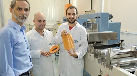
This factory is different in other ways, too. “We do not weld; we have no rivets, no screws and no bolts. We just glue components together,” says Ulrich Kranz, the head of the division that since 2013 has been making BMW’s i3 and i8 electric and hybrid vehicles in Leipzig. Since the carbon-fibre body provides the vehicle with its strength, the outer panels are mainly decorative and made from plastic. These are simple to spray in a small paint booth, whereas metal requires elaborate anti-corrosion treatment in a giant and costly paint shop. In all, the i3 factory uses 50% less energy and 70% less water than a conventional facility.

The i-series are upmarket cars, but still produced in volume. BMW has succeeded in taking a new material hitherto used in low-volume specialist applications, such as aerospace and defence, and turning it into something close to mass-produced. That called for radical changes. When in 2007 the BMW board asked Mr Kranz to come up with an electric city car and a low-energy production system, he and his team went into hiding to allow ideas to flow freely.

Mr Kranz’s material of choice was carbon fibre, not least to offset the weight of the battery. The material is made from thin filaments of carbon woven into a cloth. This is cut and pressed into the shape of a part and the fibres bound together with a plastic resin, cured by heat and pressure. The molecular structure of carbon compounds produces strong chemical bonds, much like those in diamonds, and by aligning the fibres at different angles the strength of a component can be reinforced exactly where needed.

The resulting structure, although stronger than steel, is at least 50% lighter, and also about 30% lighter than aluminium. Nor does it corrode. But in the past the production process was expensive, slow and labour-intensive. That may not matter too much when making fighter jets or Formula 1 racing cars. But even aircraft-makers had to speed things up and bring down costs when they started making passenger jets from carbon fibre.

Look, few hands

These days carbon fibre makes up about half the weight of aircraft such as the Boeing 787 Dreamliner or the Airbus A380 and A350. Lighter aircraft burn less fuel and thus have lower emissions. They can also carry more passengers and fly farther. There are economies in manufacturing, too, because large sections of the aircraft can be made in one go instead of having to join together lots of smaller aluminium panels. Aircraft-makers have found ways to speed up some of the production process, but it is still too slow and expensive for high-volume carmakers.

The answer that BMW came up was a different sort of factory and a new supply chain. It begins in Otake, Japan, with a joint venture between SGL group, another German company, and Mitsubishi Rayon. This produces what is called a precursor, a polyacrylonitrile thermoplastic, which looks a bit like fishing line wound onto large spools. This is shipped across the Pacific to Moses Lake in Washington state, the site of another joint venture, this one between BMW and SGL. The location was chosen because it uses locally generated emission-free hydroelectric power.

Black carpet

The precursor is passed through a series of heating stages in which it is carbonised into blackened filaments only around 7 micrometres (millionths of a metre) in diameter. Some 50,000 of these filaments are bundled together into a thicker strand and wound onto reels, much like a yarn in a textile factory. The tows, as the carbonised yarns are called, then cross the Atlantic to another BMW-SGL joint venture, at Wackersdorf near Munich. Here they are woven into sheets and layered into stacks that resemble carpets.

When the stacks arrive at the Leipzig factory, they are heated and pressed into a three-dimensional “preform”. Various preforms are placed together to make up large structures, which together are pressed again, but this time resin is injected into the mould, bonding and curing the final component inside the press tool. This usually happens within minutes, though in some aerospace factories the curing can take the best part of a day and requires a pressurised oven called an autoclave. Robots move the parts around and glue them together to make the main body structure of the car. Further along the production line the body is mated to the drive module, which incorporates an aluminium chassis, electric motor, battery and other components.

Mr Kranz expects carbon fibre to be used more widely in cars, but thinks they will always contain a mix of materials. BMW’s new 7 series executive car now has some carbon-fibre parts as well. Other carmakers are starting to use the material, and Apple, which has hinted that it plans to build an electric car, has reportedly been talking to BMW about carbon-fibre construction. Anthony Vicari, an analyst with Lux Research, a Boston consultancy, predicts that by the mid-2020s carbon fibre will be widely adopted in carmaking.


But not without a battle. As in other industries, traditional materials are getting better, too. Aluminium suppliers are developing new alloys. “Aluminium is the incumbent and these guys are pushing like hell or they will lose their entire industry,” notes Jean Botti, the chief technical officer of Airbus. Alcoa, a leading producer of aluminium, is developing a number of lightweight alloys. One of them, Micromill, is easier and faster to shape into intricate forms. Ford has begun using it to replace some steel components in its F-150 pickups, one of its best-selling models in America.

The upshot is that manufacturers are being offered a wider choice of materials than they had before, says Mr Botti. Carbon fibre has done wonders in aerospace, he reckons, but it is used largely in the bigger, long-range aircraft, of which only a handful might be built every month. To increase the use of carbon fibre in smaller aircraft, aerospace firms have to speed up production and bring down costs further, but “there are new techniques we are thinking about which could tremendously reduce the cost of carbon fibre.” Airbus and Boeing both have plans to raise production of their workhorse short-haul aircraft, respectively the A320s and 737s, to an astonishing 60 or so a month to meet order backlogs. Still, he cautions, companies should always take care to select the best material for a particular job. If Airbus were to replace the A320 with a new model, he says, he would have to look carefully to see if carbon fibre provided the best value in a short-haul aircraft.

Airbus is also developing its own new materials. One of these is a proprietary aluminium-magnesium-scandium alloy called Scalmalloy. It is particularly good for making lightweight high-strength components. It is being commercialised by an Airbus subsidiary and is already used in some racing cars. In powder form, Scalmalloy can also be employed in a revolutionary form of manufacturing that is ideally suited to working with many new materials: additive manufacturing, popularly known as 3D printing

3D printing: Print me a pavilion
Additive manufacturing is a perfect way of using new materials
CARMAKERS can spend a year building a working prototype for a new car. Setting up machines for a production run of one is laborious and costly, since much of the work is done by hand. But researchers in Tennessee have an automated system endearingly known as BAAM (Big Area Additive Manufacturing). Most people would call it a 3D printer, albeit a particularly large one—and it is used to print cars.

The researchers work at the Oak Ridge National Laboratory, which is exploring a number of advanced manufacturing methods. BAAM was cobbled together from various bits of factory kit in partnership with Cincinnati Inc, a machine-tool company. In one experiment it made most of the body and chassis for an electric replica of a Shelby Cobra, a classic 1960s sports car. The printed parts that went into the vehicle were built up using a mixture of 80% polymer and 20% carbon fibre and weighed a mere 227kg. It took the team just six weeks to design, print and assemble the car.

A few companies, such as Local Motors, a firm based in Phoenix, are using additive technologies to make limited runs of cars, but 3D printing is still too slow for mass-produced vehicles. Even so, it will quickly become part of the automobile industry, says Thom Mason, director of Oak Ridge, not just for prototyping or customising vehicles but also for making moulds, tools and dies. That business had been largely offshored to low-wage countries. “Now we can print these things overnight,” explains Mr Mason.
Making things with 3D printers has captured the public imagination. In recent years, improved hardware and software has turned the basic technology—which is about 20 years old—into a broad assortment of different processes. They all rely on building up layers of material additively, using plastics, metals, ceramics and even biological feedstocks. Such printers range from desktop machines that cost a few thousand dollars to hulking monsters to print metal parts that cost over $1m.

The size of what could be printed used to depend on what would fit inside the machine. Now some printers, such as BAAM, are coming out of the box, so to speak. MX3D, a Dutch startup, plans to print a 15-metre (49-foot) footbridge across a canal, using robots fitted with steel-printing equipment. Winsun, a Chinese firm, uses a fast-drying mixture of cement and recycled construction waste to print prefabricated sections of buildings, and Achim Menges at the University of Stuttgart is printing strands of carbon fibre to make one-off architectural structures such as pavilions (pictured).

Strand by strand

One of a kind

One advantage of producing something additively is that material is deposited only where needed, so there is little waste. In traditional manufacturing perhaps 80% of the material is cut away. Moreover, the software used to design a product can also run the printer. And software is easy to tweak, so a different design can be produced every time without having to reset machines. The technique also lends itself to making complex shapes in new materials that can lead to dramatic performance gains. And although 3D printing is still slow compared with mass-production processes such as pressing steel and plastic injection moulding, in some industries that may not matter too much.

“Additive techniques give you a whole new degree of freedom,” says Mr Idelchik at GE Research. The company has spent $50m installing a 3D printing facility at a plant in Auburn, Alabama, to produce fuel nozzles for the new LEAP jet engine it is making in partnership with Snecma, a French company. GE will begin by printing 1,000 nozzles a year, but eventually the number could reach 40,000. The fuel nozzle in a jet engine is a complex part that has to withstand high temperature and pressure. Normally it is made from 20 different components. GE instead prints the part in one go, with a laser fusing together layers of a powdered “super alloy” made up of cobalt, chrome and molybdenum. The resulting nozzle is 25% lighter and five times more durable than the old sort, and conventional manufacturing methods might not have been able to cope with the material at all.

“Additive manufacturing will definitely win a lot of ground at the expense of existing processes,” says Henrik Runnemalm, the head of engines for GKN Aerospace, a British company. Some of GKN’s 3D-printed components are already in aircraft and jet engines. The technology is also used alongside traditional techniques. Mr Runnemalm cites an example in which a fine wire of material is melted to build up shapes on a component that has been cast in a conventional manner. In yet another process, a 3D printer creates a component in its “near-net shape” (close to its final form), which is then finished conventionally with machine tools.
Additive manufacturing has plenty of potential left, not least because it can change the properties of materials as it goes along. At Oak Ridge, researchers are working on specifying the crystalline structure of a metal in different parts of a component by fine-tuning the heat as the layers are built up, hoping to obtain different performance characteristics. “This is totally new,” says Mr Mason. “It is one of those things that is not in our design vocabulary right now.”

3D printing is capable of even more. Modumetal’s nanolaminates are also produced by additive manufacturing. The process takes place close to room temperature, which means metal could be added to a 3D-printed plastic shape, creating hybrid plastic-metal composites, says Ms Lomasney. And the process could run in reverse, dissolving the metal in a component back into a solution so that it could be used again. “We haven’t got into the business of recycling because parts are not yet being returned to us,” explains Ms Lomasney, “but in theory it’s possible.” With many new materials, recycling may become an essential requirement.

What next: Bright angelic mills
Though recycling will become more complicated, a much wider choice of materials will transform manufacturing

MANUFACTURERS are coming under growing pressure to take responsibility for the life cycle of their products. This involves an obligation to consider all the energy, environmental and health effects of every stage, from materials extraction to production, distribution and, eventually, recycling or disposal. As materials become more complex, that is becoming trickier.

The traditional way of gauging what effects a new material will have on the wider world is to go by the elements. If something has lead in it, for instance, it is probably not good for you. If it has a bit of manganese, it is probably safe. “That is so old-fashioned,” says Berkeley’s Mr Ceder. “Very often what these things do to your body depends on the form, not the chemistry.”

That makes nanoparticles particularly difficult. A lot of research is being done on their environmental and health implications, but much of it is inconclusive. A big five-year study of nanoparticles led by the Swiss National Science Foundation is due to be published in 2016. One example of its work, from Australia, illustrates the concerns.
Being a highly developed region, South Australia gets plenty of nanoparticles in products, some of which are washed into the drainage system. It is a dry place, so much of the wastewater is recycled, and treated sewage is used to fertilise fields. That allowed researchers from the Swiss Federal Laboratories for Materials Science and Technology to study the area as something of a closed system. From field and water deposits, they calculated the amounts of four nanomaterials that ended up in the environment every year: 54 tonnes of nano titanium dioxide (used in sunscreens); 10 tonnes of nano zinc oxide (found in cosmetics); 2.1 tonnes of carbon nanotubes (hollow tubes used instead of fibres in some composites); 180 kilograms of nano silver (for anti-bacterial use); and 120kg of fullerenes, another nano form of carbon, made up of hollow spheres known as “buckyballs”.

The final destination of these particles varied. The nano carbons remained embedded in the parts they came in, which ended up in rubbish dumps. The zinc oxide and silver were chemically converted into normal compounds in sewage-treatment plants, so did not seem to present a risk. But the nano titanium dioxide from sunscreens went walkabout. Just over 5% ended up in the sea, the rest on fields. In its normal form titanium dioxide is not toxic (it is used in toothpaste as well as sunscreen), but the researchers say they do not know what the long-term effects of the nano versions will be, especially in high concentrations.
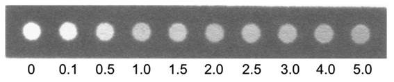
Going dotty

Certain nanoparticles undoubtedly have nasty effects. Some LEDS use quantum dots—tiny crystals which when excited by an external light source glow brightly, a process called luminescence. This produces richer lighting and brighter colours in LED televisions and other displays. The dots, though, are often made from a toxic cadmium compound. That provides a commercial incentive to come up with safer materials.
Loking for the perfect LED

Nanoco, a firm based in Manchester, has developed cadmium-free quantum dots. The Dow Chemical Company has licensed the technology to make dots at a new factory in South Korea. And Prashant Sarswat and Michael Free of the University of Utah have made quantum dots out of carbon obtained from food waste. This is put into a solvent and heated under high pressure. The process still needs to be scaled up, but as the raw ingredients are free and relatively safe, the idea has promise.

For larger items, the end-of-life problems are just as challenging—and rather more visible. Both Airbus and Boeing have programmes for recycling their carbon-fibre aircraft. In that industry at least the numbers are limited to a few thousand, but if carmakers were to adopt carbon fibre on a larger scale, millions of old carbon-bodied cars would eventually have to be disposed of. In some cases the material can be shredded and used in lower-grade components.

Recycling exotic materials might become a necessity. Some elements are expensive and hard to find; they may come from only a handful of countries, such as China, which could restrict supply. Others, including some rare earths, are not found in large quantities and are hard to mine. Such substances are being increasingly used in electric and hybrid cars. As these become more widespread, new methods of dismantling and recovering materials will have to be found.

Marion Emmert and H.M. Dhammika Bandara at Worcester Polytechnic Institute in Massachusetts have developed a new and energy-efficient way to extract rare-earth elements from electric cars, in particular neodymium, dysprosium and praseodymium. They sliced up and shredded the motor and other drive components from an all-electric Chevrolet Spark and used a two-stage chemical-extraction method to separate the rare earths and other useful materials. The technology, they say, could be used for other products that contain motors and magnets, such as wind turbines and medical imaging equipment.

Some firms use a process called life-cycle assessment (LCA) to work out environmental impacts. “The idea is to evaluate, cradle to grave, a product or service,” says Christian Lastoskie, an expert in the field at the University of Michigan. LCA used to be carried out when a product had been on the market for a while and plenty of data were available. Now it can be done in advance with computer modelling. That means making and testing a number of assumptions about a new material or process, but the analysis can be a useful guide to possible environmental concerns and help a company with its selection of materials, Mr Lastoskie explains.

One project he has worked on, with backing from Sakti3, was a comparison of the life cycle of conventional lithium-ion batteries and solid-state ones. The results, published in 2014 in the Journal of Cleaner Production, suggested that even after allowing for uncertainties about the properties of the cells and the efficiency of the process used to make them, the use of solid batteries in electric vehicles would bring down energy consumption and reduce global warming.

All this points to the conclusion that manufacturing will become ever more complex and that the days of “me-too” factories, making similar products in much the same way, are numbered. Processes such as 3D printing make economies of scale irrelevant, allowing low-volume production and rapid customisation. As labour costs shrink in relation to total production costs, there is less pressure to move production to low-wage countries. That does not mean foreign companies will give up making things in China, but that more of the things they make there will be for the Chinese.

With computing costs falling all the time, being able to model the manufacturing process and the life cycle of a new material opens up markets to new entrants with new ideas. Only a decade ago it was widely thought that the world’s car industry would consolidate into less than half a dozen groups because the barriers to entry were so high. Now new carmakers are appearing everywhere; not just Tesla and, possibly, Apple, but also many small, specialist ones such as Local Motors.

Big companies, too, will increasingly compete by using exclusive recipes for new materials and customised production techniques. “If you just do a great design and use a manufacturing process which everyone else can use, you will run out of steam,” says Mr Idelchik at GE Research. “But if you have a proprietary manufacturing process which applies to proprietary materials, you are creating a long-lasting competitive differentiation.”

Trade secrets

Mr Idelchik is not alone in that view. BMW’s factory in Leipzig uses standard industrial equipment and robots. What makes it special is the company’s intimate knowledge of exactly how its materials are made and how to control the processes that turn them into cars. This goes to the heart of materials science. “We think we are pretty much ahead of our competitors because we have the complete process and material development in our hands,” says BMW’s Mr Kranz.

In future more firms will need to be on top of their materials. The days of trial and error are coming to an end as powerful research tools deliver scientific data of unprecedented depth. The tumbling cost of computer power makes that information available to companies of all sizes just as new production processes, such as 3D printing, transform the economics of manufacturing into something lighter and swifter.

Mastering the greater complexity of materials, as well as their design, engineering, production, supply-chain and life-cycle management, will require new skills and plenty of entrepreneurial talent. It may attract more people into an industry that is still trying to shake off an image of dark satanic mills. Manufacturing is entering a new age. Edison would have heartily approved.

Fonte: The Economist

RAND Corporation Assesses NIOSH Nanotechnology Research Center


The National Institute for Occupational Safety and Health (NIOSH) posted a RAND Corporation (RAND) report entitled Nanomaterial Safety in the Workplace:  Pilot Project for Assessing the Impact of the NIOSH Nanotechnology Research Center.  

In August 2014, NIOSH asked RAND to help develop and apply a method for assessing its Nanotechnology Research Center’s (NTRC) contribution to improving the safety and health of workers who could be affected by the production, use, reuse, or disposal of the products of nanotechnology that are of greatest concern to workers, such as engineered nanomaterials.  

The report describes the method used to construct the NTRC logic model and includes “insights and guidance” for gathering and organizing information about NTRC’s operations and their impact on or contributions to worker safety and health.  

The report states that RAND, in coordination with NTRC leadership, identified a portion of the NTRC to pilot the method and search for evidence of NTRC’s activities and outputs that contribute to worker safety and health.  For purposes of the pilot study, RAND limited its data collection concerning NIOSH outputs and stakeholder engagement to information and organizations associated with nano-titanium dioxide and nano-silver.  

RAND identified a set of common categories of NTRC activities and outputs, as well as classes of stakeholders, including workers and industrial, advocacy, governmental, research, educational, and training organizations, each of which uses NTRC’s outputs in ways that could contribute to NIOSH’s mission.  RAND also identified, with input from NTRC leadership, a small number of external customers and intermediate parties with whom to discuss NTRC’s outputs and services and how they are used to affect worker safety and health.  

RAND states that the discussions identified potential factors that might be inhibiting NIOSH’s ability to achieve its desired outcomes.  For example, according to the report, “there is often not an explicit connection between the exposure to a particular nanomaterial, the health effect of that exposure, and the specific steps that should be taken in response to that exposure.”  The report states that “the pace at which new nanomaterials are being developed and used by industry appears to exceed the pace of safety and health research and regulations, which can lead to outdated and insufficient rules,” and that the “lack of formal regulations may be limiting the use of on-site exposure monitoring.”  

The report notes that “premature regulation based on inadequate research and data may not be well received by NTRC customers and intermediate parties,” however.  RAND concludes that “[a] more comprehensive review of NTRC across industry sectors, NIOSH-defined critical topic areas, and engineered nanomaterials or nanotechnologies is necessary to more fully characterize the breadth and scope of NTRC’s success and barriers to achieving impact.”

Fonte: NanoTech LawBC

Nanomaterial with the potential to mop up giant oil spills

A common cosmetics ingredient is being developed into a nano-material with the potential to mop up giant oil spills. Viviane Richter explains. 
When BP’s Deepwater Horizon oil rig exploded in 2010 it dumped more than 300 Olympic swimming pools of oil into the Gulf of Mexico. Cleaning up a massive spill involves burning off the oil, or using chemicals to break up the slick and disperse it through the oceans.
A new material made from a common cosmetics ingredient could pick up the oil and remove it from the sea, much like blotting up a kitchen spill with a paper towel. The material was described by a team led by nanotechnologist Ian Chen of Deakin University in Geelong in Nature Communications in November.
Chen’s material is made from sheets of boron nitride, or “white graphite”, which is used in cosmetics to stop powders clumping and to soak up oils on skin.
Chen's oil-absorbent sheets (left) are stable at high temperatures (right).CREDIT: IAN CHEN, DEAKIN UNIVERSITY
“[The new sheets] will change the way people utilise boron nitride,” says David Officer, organic chemist at the University of Wollongong.
At the nano-level, boron nitride consists of single-atom-thick layers, stacked like pages in a newspaper. Ordinarily only the outermost layers trap oil, limiting the material's absorptive capacity.
The team has boosted that capacity by separating the boron nitride layers, scrunching them up, and then reassembling them into sheets that can be thrown over floating oil.
The boron nitride is first treated with urea to separate the layers, and the solution is  shredded through an industrial grinder. The torn and separated boron nitride layers pucker and join as they dry, forming sheets five times thinner than a piece of paper. So far Chen has produced sheets the size of a post-it note, but with a huge surface area for sopping up oil. A single gram of the sheets, spread out flat, would cover five tennis courts.
Dark and light brown crude oil from the Deepwater Horizon rig floats on the surface of the Gulf of Mexico. Chemical dispersants used to treat the oil spill are also damaging to the environment.CREDIT: KRIS KRÜG/GETTY IMAGES
What’s more, the sheets are stable to 800°C, raising the possibility that oil could be burnt off in furnaces and the material used again. This gives it an advantage over another candidate material: raw cotton. Cotton can mop up to 36 times its own weight in oil, but once used it has to be tossed. Another promising candidate, graphene – a chemical cousin of boron nitrate – absorbs up to 86 times its weight in oil but is less stable at high temperature, limiting its reuse.
And even though the Chen team is still testing the absorption power of the boron nitride sheets, the method has already mopped up interest from industry – a textile company is working with Chen to find ways to produce much larger films.
Officer is optimistic this can be done. “[The sheets] are an excellent material for fabrication,” he says.
Viviane Richter is a staff writer at COSMOS.

Fonte: Cosmos

Nanotecnologia para a medição de vitamina C


O Brasil é o maior produtor e exportador mundial de suco de laranja. Segundo o Ministério da Agricultura, o país é responsável por 30% da safra anual da fruta e por 60% da produção mundial de suco, da qual mais de 90% é exportada. Para avaliar a qualidade deste suco, um dos parâmetros é a concentração da substância chamada ácido ascórbico. Popularmente conhecido como Vitamina C, o ácido ascórbico está presente naturalmente numa enorme variedade de alimentos e ainda é usado amplamente como conservante em diversas aplicações industriais.
Assim, pesquisadores do Laboratório Nacional de Nanotecnologia (LNNano), do Laboratório Nacional de Luz Síncrotron (LNLS), e dos Institutos de Química da Universidade Estadual de Campinas (UNICAMP) e da Pontifícia Universidade Católica de Campinas (PUCC) desenvolveram um método simples e rápido para a medição do conteúdo de ácido ascórbico em determinadas amostras por meio de um sensor feito a partir da deposição de nanopartículas de prata sobre um papel cromatográfico.

Vitamina C 
O ácido ascórbico exerce um papel importante no metabolismo de animais e plantas e é produzido naturalmente pela grande maioria deles. No entanto, algumas espécies de peixes, morcegos e primatas – incluindo os seres humanos – não são capazes de produzi-lo e precisam adquirir essa vitamina a partir da alimentação.
Nos mamíferos, o ácido ascórbico é um componente importante para produção do colágeno, a principal proteína constituinte do tecido conjuntivo. A falta de ácido ascórbico leva à má formação desta proteína, o que provoca a doença chamada escorbuto, cujos sintomas incluem hemorragias nas gengivas, dores nas articulações e dificuldades de cicatrização.
Apesar de muito comum no passado, deficiências de vitamina C são cada vez mais raras, tanto pela maior disponibilidade de alimentos ricos nessa vitamina, quanto pela adição de ácido ascórbico como conservante em alimentos industrializados.
Além da indústria alimentícia, o ácido ascórbico também é usado como conservante nas indústrias farmacêutica, química e cosmética devido a suas propriedades antioxidantes. A determinação da concentração do ácido ascórbico é, assim, importante para o controle de qualidade destes produtos. No entanto, métodos comuns de aferição da quantidade de ácido ascórbico exigem sofisticado aparato experimental e ambiente laboratorial, grandes quantidades de reagentes e tempo para a execução dos experimentos, o que, muitas vezes, não é conveniente para as aplicações industriais.

Nanopartículas de Prata
Com foco na portabilidade e na redução de custos, os cientistas desenvolveram seu método a partir de um item bastante comum em laboratórios: o papel cromatográfico. Normalmente usado na separação de compostos químicos, aqui o papel é usado como suporte para um reagente colorimétrico, formando um sensor que muda de cor em contato com diferentes concentrações de uma substância.
Como reagente colorimétrico, os pesquisadores utilizaram nanopartículas de prata, obtidas a partir de nitrato de prata (AgNO3), e depositadas sobre uma região preparada no papel cromatográfico. A seguir, este sensor baseado em papel foi colocado em contato com soluções de diferentes concentrações de ácido ascórbico. Verificou-se que, ao entrar em contato com o ácido, a região contendo as nanopartículas não só muda de cor, como a mudança depende da concentração de ácido ascórbico nas soluções.
Figura: Resposta colorimétrica do sensor baseado em papel cromatográfico com nanopartículas de prata para concentração de ácido ascórbico variando entre 0 e 5 mmol.L-1 (milimols por litro). Quando maior a concentração de vitamina C, maior a mudança de cor no sensor.

Através da técnica de espalhamento de raios-x a baixos ângulos (SAXS) da linha de luz SAXS1 do LNLS, os pesquisadores puderam investigar o tamanho médio e a distribuição das nanopartículas, antes e depois da exposição ao ácido ascórbico. Verificou-se um aumento no tamanho médio das nanopartículas, o que indica que, ao entrar em contato com soluções contendo ácido ascórbico, as nanopartículas agiram como núcleos para a transformação dos íons de prata em prata metálica devido às propriedades antioxidantes do ácido. O aumento do tamanho das nanopartículas é o que modifica a cor do papel cromatográfico e o que permite desenvolver uma escala colorimétrica para a concentração de ácido ascórbico.
Segundo uma das autoras da pesquisa, Gabriela Furlan Giordano, a vantagem deste método começa na rapidez com que as análises são executadas: ”em trinta minutos nós conseguimos ter as respostas de oito amostras no colorímetro, que é um instrumento portátil e de baixo custo”, além de gerar menos resíduos devido ao menor uso de reagentes.
Por fim, os pesquisadores argumentam que o sensor baseado em papel é sensível e preciso para aplicações em amostras não-biológicas. Ainda, a portabilidade e manutenção da qualidade de medição por semanas, sob refrigeração e na ausência de luz, demonstra seu grande potencial para a aplicação em sensores comerciais.
A pesquisa foi desenvolvida com suporte da Fundação de Amparo à Pesquisa do Estado de São Paulo (FAPESP).
Fonte: D.C.M. Ferreira, G.F. Giordano, C.C.S.P. Soares, J.F.A. de Oliveira, R.K. Mendes, M.H. Piazzetta, A.L. Gobbi, M.B. Cardoso, Optical paper-based sensor for ascorbic acid quantification using silver nanoparticles, Talanta 141 (2015) 188-194, doi:10.1016/j.talanta.2015.03.067.

Sobre o LNLS
O Laboratório Nacional de Luz Síncrotron (LNLS) integra o Centro Nacional de Pesquisa em Energia e Materiais (CNPEM), uma organização social qualificada pelo Ministério da Ciência, Tecnologia e Inovação (MCTI). Localizado em Campinas (São Paulo), o LNLS é responsável pela operação da única fonte de luz sincrotron da América Latina, aberta ao uso das comunidades acadêmica e industrial. O sincrotron brasileiro possui hoje 18 estações experimentais – chamadas linhas de luz –, voltadas ao estudo de materiais orgânicos e inorgânicos por meio de técnicas que empregam radiação eletromagnética desde o infravermelho até os raios X.
O LNLS está neste momento construindo o Sirius, uma fonte de luz sincrotron de quarta geração, planejada para ser uma das mais avançadas do mundo. Sirius abrirá novas perspectivas de pesquisa em áreas como ciência dos materiais, nanotecnologia, biotecnologia, física, ciências ambientais e muitas outras.

Sobre o LNNano
O Laboratório Nacional de Nanotecnologia (LNNano) está localizado em Campinas-SP e é integrante do Centro Nacional de Pesquisa em Energia e Materiais (CNPEM), uma organização social qualificada pelo Ministério da Ciência, Tecnologia e Inovação (MCTI). O Laboratório, aberto a usuários, busca, por meio de pesquisa in house, explorar oportunidades oferecidas pela nanotecnologia para atender às necessidades da agricultura, indústria e serviços, em âmbito regional, nacional e internacional. O LNNano também atua na criação e desenvolvimento de produtos e processos sustentáveis, através de seus cinco laboratórios: de Microscopia Eletrônica, de Microfabricação, de Ciência de Superfícies, de Materiais Nanoestruturados e de Caracterização e Processamento de Metais.
Fonte: CNPEM